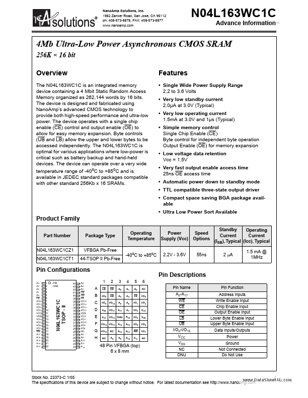
N04L163WC1C
Key Features
- Single Wide Power Supply Range 2.2 to 3.6 Volts
- Very low standby current 2.0µA at 3.0V (Typical)
- Very low operating current 1.5mA at 3.0V and 1µs (Typical)
- Simple memory control Single Chip Enable (CE) Byte control for independent byte operation Output Enable (OE) for memory expansion
- Low voltage data retention Vcc = 1.5V
- Very fast output enable access time 25ns OE access time
- Automatic power down to standby mode
- TTL compatible three-state output driver
- Compact space saving BGA package available
- Ultra Low Power Sort Available Product Family Part Number N04L163WC1CZ1 N04L163WC1CT1 Package Type VFBGA Pb-Free 44-TSOP II Pb-Free Operating Temperature -40oC to +85oC Power Supply (Vcc) 2.2V - 3.6V Speed Options 55ns Standby Operating Current Current (ISB), Typical (Icc), Typical 2 µA 1.5 mA @ 1MHz